working of photo sensor
- time:2025-07-26 00:30:47
- Click:0
Unlocking Light: How Photo Sensors Translate Photons into Pixels and Data
Have you ever wondered how your smartphone instantly captures a vibrant sunset, how your garage door knows not to close on your car, or how medical scanners peer inside the human body? The remarkable technology enabling these feats, often hidden in plain sight, is the humble yet sophisticated photo sensor. These electronic eyes are the fundamental components converting the invisible dance of light particles into the digital signals that shape our modern world. Understanding the working of photo sensors reveals a fascinating interplay between physics and engineering, transforming fleeting photons into actionable information.
At its core, the working of a photo sensor hinges on the photoelectric effect, a principle famously explained by Albert Einstein. When a particle of light, called a photon, strikes certain materials (primarily semiconductors like silicon), it can transfer its energy to an electron within that material. If the photon’s energy is sufficient (which depends on its wavelength or color), it liberates the electron, creating a free electron and a corresponding positively charged “hole.” This basic generation of charge carriers (electrons and holes) is the crucial first step in the photodetection process.
The most common building block for modern photo sensors is the photodiode. A photodiode is essentially a semiconductor P-N junction (where a P-type material rich in holes meets an N-type material rich in electrons) designed specifically to be sensitive to light. Typically, this junction is reverse-biased during operation, meaning a voltage is applied to widen the depletion region – an area naturally devoid of free charge carriers near the junction.

Here’s the magic:
- Photon Absorption: When light penetrates the photodiode’s surface and reaches the depletion region (or areas close enough for carriers to diffuse into it), photons are absorbed.
- Electron-Hole Pair Generation: Each absorbed photon generates an electron-hole pair through the photoelectric effect.
- Charge Separation & Drift: The inherent electric field within the depletion region acts as a powerful force. It sweeps the negatively charged electron towards the N-side and the positively charged hole towards the P-side of the junction.
- Current Flow: This movement of separated charges constitutes a photocurrent. Crucially, the intensity of the incident light directly correlates with the number of photons absorbed and thus the *magnitude of the photocurrent generated*. Brighter light means more photons, which means more electron-hole pairs, resulting in a stronger electrical current.
While the photodiode provides the fundamental light-to-current conversion, turning this raw signal into usable digital data (like a photograph) requires further sophisticated processing. This is where image sensors come into play, consisting of arrays of millions, or even billions, of microscopic photodiodes – each acting as a single pixel.
Two dominant technologies perform this crucial signal conversion and readout in digital imaging:
- CCD (Charge-Coupled Device): Imagine a bucket brigade. In a CCD sensor, the tiny electrical charge packets (representing light intensity) generated by each pixel’s photodiode are physically transferred, bucket-by-bucket, across the silicon chip to a single corner. Here, a dedicated amplifier converts the accumulated charge into a voltage signal. This serial readout method allows for very precise charge transfer with minimal noise interference, historically offering high image quality. However, it consumes more power and operates slower than its counterpart. CCDs are still favoured in applications demanding ultimate precision and low noise, like astronomical telescopes or high-end scientific cameras.
- CMOS (Complementary Metal-Oxide-Semiconductor): Modern CMOS sensors (often termed CMOS Active Pixel Sensors) adopt a fundamentally different, parallel approach. Crucially, each pixel in a CMOS sensor contains its own miniature amplifier circuit, right next to the photodiode. This allows each pixel’s signal to be amplified at the source. Furthermore, CMOS sensors leverage sophisticated transistor switches within each pixel, enabling the direct addressing of individual pixels or entire rows/columns simultaneously. This parallel readout architecture grants CMOS sensors significant advantages: drastically lower power consumption, faster readout speeds (enabling high frame rates for video), lower manufacturing costs (compatible with standard chip fabrication), and the potential for integrating more processing circuitry directly on the sensor chip. These benefits make CMOS the overwhelmingly dominant technology in smartphones, digital cameras, webcams, and countless other applications.
The journey from light to data involves several key stages after the initial photon detection:
- Charge-to-Voltage Conversion: Whether amplified at the pixel (CMOS) or after serial transfer (CCD), the minute photocurrent or stored charge is converted into a proportional voltage signal.
- Amplification: This voltage signal is extremely weak and requires significant amplification to be processed reliably. This happens at the pixel level in CMOS and at the output node in CCDs.
- Analog-to-Digital Conversion (ADC): The amplified analog voltage signal, which represents light intensity continuously, must be converted into discrete digital numbers (binary code) that computers and displays can understand. In many CMOS sensors, ADCs are integrated onto the chip itself, even located on the sensor’s column lines for faster processing.
- Digital Signal Processing (DSP): The raw digital data undergoes significant processing – correcting for imperfections, adjusting color balance, applying noise reduction, and compressing the image data – before becoming a usable JPEG or video frame. This often happens either on the sensor chip or in a dedicated image processor.
The working of photo sensors enables a staggering array of applications far beyond capturing selfies:
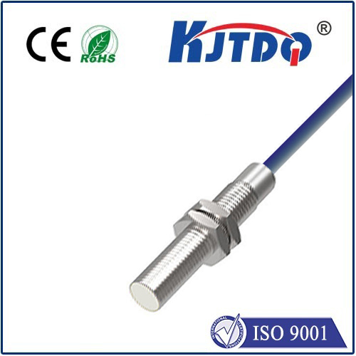
- Consumer Electronics: Digital cameras, camcorders, smartphone cameras, barcode scanners, optical mice, ambient light sensors.
- Industrial Automation: Object detection and counting, position sensing, quality control inspection, robotics guidance.
- Scientific & Medical: Spectroscopy, microscopy, endoscopes, pulse oximeters, X-ray detectors (using specialized sensors), DNA sequencers.
- Automotive: Lane departure warning, adaptive headlights, night vision cameras, autonomous vehicle perception systems (LiDAR, cameras).
- Security & Surveillance: CCTV cameras, motion detectors, biometric scanners.
From the fundamental photoelectric effect liberating electrons within a photodiode to the complex orchestration of charge transfer, amplification, and digitization in CCD and CMOS image sensors, the working of photo sensors is a triumph of physics and microelectronics. These intricate devices act as vital translators, continuously converting the ubiquitous energy of light into the digital language of information that powers innovation across countless fields, silently shaping our interaction with the physical world. Their ability to precisely measure light intensity and capture detailed images forms the bedrock of modern visual technology.